Developer Offer
Try ImaginePro API with 50 Free Credits
Build and ship AI-powered visuals with Midjourney, Flux, and more — free credits refresh every month.
AI Supercharges Quantum Chip Defect Detection
The Quantum Scaling Challenge A Need for Speed and Precision
Quantum computing (QC) holds the promise of solving problems far beyond the reach of today's most powerful supercomputers. But to unlock this potential, we need to scale up quantum processors, which involves building complex 3D architectures. Just like in traditional microchips, this move towards miniaturization and 3D integration in quantum devices—especially those based on ion traps—is critical for boosting performance.
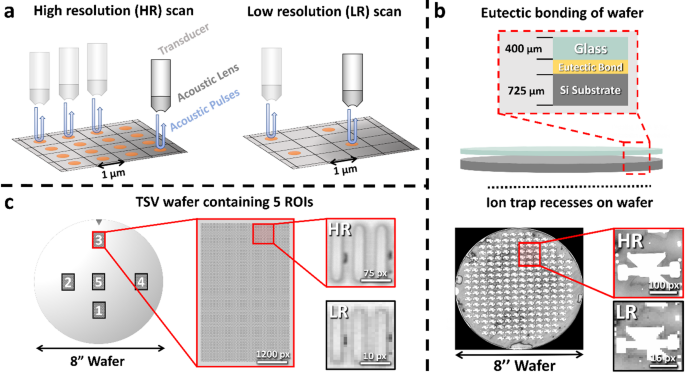
However, this complexity introduces significant manufacturing challenges. The processes for creating these structures, such as wafer-to-wafer bonding and fabricating through-silicon vias (TSVs) that act as vertical electrical connections, are incredibly delicate. Even the tiniest imperfections, like voids, cracks, or poor adhesion, can cause an entire device to fail. Finding these microscopic defects is crucial for quality control and improving production yields.
The go-to method for this task is Scanning Acoustic Microscopy (SAM), a non-destructive technique that uses sound waves to see inside the chip. The problem? Achieving a high enough resolution with SAM to spot tiny defects across an entire wafer is extremely time-consuming and expensive. There's a fundamental trade-off: higher resolution means longer scan times. This bottleneck makes it impractical for the rapid, large-scale analysis needed for industrial production.
AI to the Rescue A Smarter Imaging Workflow
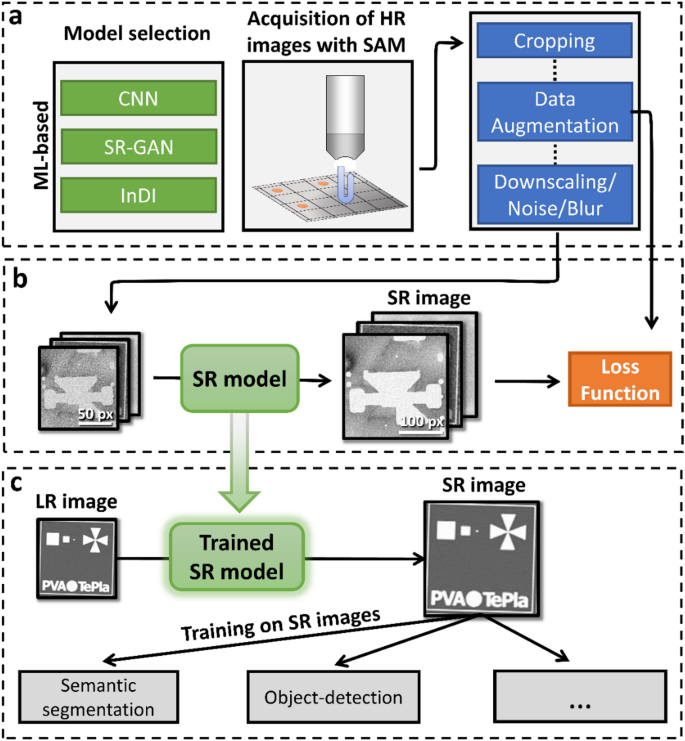
To break this trade-off, researchers have developed an innovative, fully automated workflow that combines fast, low-resolution SAM scans with the power of artificial intelligence. The core of this solution is an AI technique called super-resolution (SR).
The process is elegantly simple:
- Fast Scan: A quick, low-resolution SAM scan of the wafer is performed, capturing the necessary data in a fraction of the time a high-resolution scan would take.
- AI Enhancement: This low-resolution image is then fed into a specially trained AI model. The model intelligently enhances the image, filling in the missing details to generate a high-quality, high-resolution version. This is done through a self-supervised learning approach, where the model is trained on a vast dataset of acoustic microscopy images to understand how to realistically upscale them.
- Automated Analysis: The newly enhanced, high-resolution image is then passed to other specialized AI algorithms for automated failure analysis. These can include object detection models like You Only Look Once (YOLO) to find and classify defects in TSVs, or segmentation models like U-Net to assess the quality of wafer bonding.
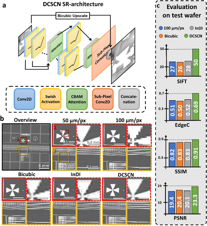
Choosing the Right AI Why DCSCN Outperforms the Rest
Not all AI super-resolution models are created equal. The research team rigorously tested several state-of-the-art architectures, including Generative Adversarial Networks (GANs) and diffusion-like models (InDI), against a deep convolutional neural network (DCSCN).
While highly generative models like GANs and InDI are powerful, they come with a significant risk: AI "hallucinations." These models can sometimes invent details that aren't present in the original data, a critical flaw when accuracy is paramount for failure analysis. Furthermore, these models are computationally expensive, requiring more powerful hardware and consuming more energy.
In contrast, the DCSCN model proved to be the ideal choice. It delivered the best balance of performance, efficiency, and reliability. It consistently produced superior-quality images without generating unphysical artifacts. The DCSCN architecture was also more time-efficient and had a lower energy footprint, making it a more practical and sustainable solution for industrial applications.
Putting it to the Test Analyzing Ion Trap Wafers
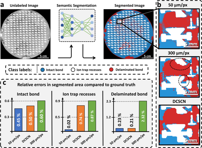
To validate the workflow, the team first analyzed an eutectically bonded wafer used for ion trap quantum devices. They compared the automated analysis of a fast, 300 µm/px scan enhanced with the DCSCN model to a slow, high-resolution 50 µm/px scan. The measurement for the high-resolution scan took six times longer.
The results were impressive. The AI-enhanced image allowed a U-Net segmentation model to accurately identify and quantify different regions—intact bonds, delaminated areas, and ion-trap recesses—with a much lower error rate than when using the original low-resolution image. The super-resolution step was critical for enabling the segmentation AI to see fine details, drastically improving accuracy while benefiting from the speed of the low-resolution scan. This combined approach cut the total analysis time by a factor of six.
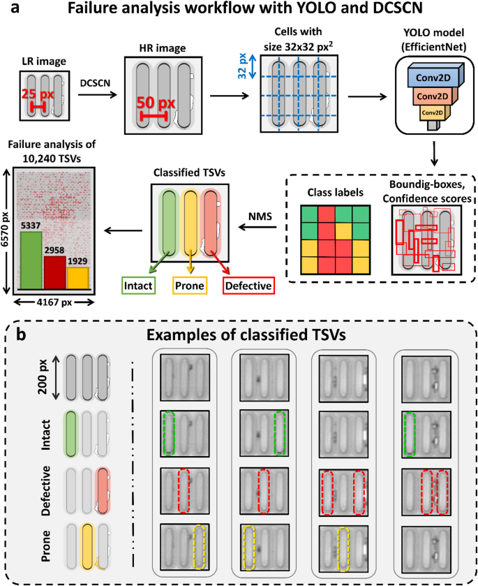
Super-Resolution Meets Super-Fast Detection for TSVs
The second test involved analyzing a wafer with over 10,000 through-silicon vias (TSVs). Detecting defects in these tiny, densely packed structures is a major challenge for object detection algorithms. In their original low-resolution state, the TSVs were too small and close together for some AI models to even process.
However, after applying the DCSCN super-resolution model, the image quality was high enough for a YOLOv2 object detection algorithm to shine. The AI could then rapidly and accurately scan the entire wafer, locating each TSV and classifying it as 'intact,' 'defective,' or 'at risk' with 99.8% detection accuracy and ~97% classification accuracy.
This workflow achieved an overall time saving of about 4x compared to traditional high-resolution scanning. Moreover, the YOLO object detection model itself was 60 times faster than previously published sliding-window techniques, demonstrating a massive leap in analytical efficiency.
A Leap Forward for Quality Control in Tech Manufacturing
This research successfully demonstrates how AI-powered image enhancement can overcome critical bottlenecks in semiconductor and quantum device manufacturing. By pairing fast scans with intelligent super-resolution, this workflow delivers high-throughput, accurate, and statistically relevant failure analysis.
The overall time savings of 4x to 6x, combined with a 60x faster detection algorithm, represents a significant advancement. This approach not only accelerates the path toward scalable quantum computing but also offers a powerful, general-purpose tool that can be applied to quality control in various high-tech manufacturing fields, ensuring higher yields, better reliability, and faster innovation.
Compare Plans & Pricing
Find the plan that matches your workload and unlock full access to ImaginePro.
| Plan | Price | Highlights |
|---|---|---|
| Standard | $8 / month |
|
| Premium | $20 / month |
|
Need custom terms? Talk to us to tailor credits, rate limits, or deployment options.
View All Pricing Details